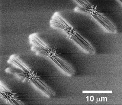
Mass-producing nanodevices may become a reality now that scientists in the US have demonstrated a new way of making millions of tiny electronic components at once.
Miniature electronic components like transistors and capacitors in computers are currently made from silicon, but they can only be made so small with existing technology. Using nanowires is one solution but growing them in the right place, in the right direction has proved challenging.
Now Babak Nikoobakht of the National Institute of Standards and Technology (NIST) has combined some conventional lithographic techniques with a new way of easily and reliably growing zinc oxide (ZnO) nanowires on a sapphire lattice.
'A [gold] nanodroplet acts as the growth site for the nanowire,' Nikoobakht explains. 'As the ZnO crystal grows on the sapphire, it pushes the gold droplet forward along the lattice structure, giving it a "preferred" direction.'

Zinc oxide nanowires grow along the lattice structure of the sapphire substrate
© Babak Nikoobakht
|
He thinks that individual nanocrystals form inside the gold droplet in a 'vapour-solid-liquid' mechanism.
Many techniques for making reliable nanodevices such as field effect transistors (FETs) or LEDs require moving individual nanowires from one surface to another - clearly not feasible for industry. The advantage of Nikoobakht's technique is that the wires are grown directly onto the surface of the chip.
Nikoobakht admits that sapphire is certainly more expensive than silicon. But on a large scales costs would come down, he says. 'Sapphire is already used as a substrate for the majority of thin film optical devices, and plays a very important role combined with ZnO in invisible circuitry and transparent displays.'
Heiko Wolf, a researcher at IBM in Zurich, Switzerland, said that the research could allow nanodevices to be made more easily. 'Up to now controlled [growth] of nanowires was only achieved on substrates of crystalline semiconductors - growing them in a predefined direction on an insulator could facilitate the fabrication of nanowire-based devices.'
But he told Chemistry World that the technique may not yet be refined enough for large-scale production. 'Industrial requirements are very stringent. The growth of individual nanowires from small pre-positioned catalytic seeds could be the next challenge to address.'
Jonathan Edwards


