РОССИЙСКАЯ АКАДЕМИЯ НАУК
УРАЛЬСКОЕ ОТДЕЛЕНИЕ
УРАЛЬСКОЕ ОТДЕЛЕНИЕ
ИНСТИТУТ ХИМИИ TBEPДОГО ТЕЛА
РОССИЙСКАЯ АКАДЕМИЯ НАУК УРАЛЬСКОЕ ОТДЕЛЕНИЕ ИНСТИТУТ ХИМИИ TBEPДОГО ТЕЛА |
|
|
| 03.07.2008 |
|
|
|
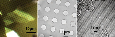
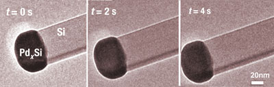
With resolution increased to this degree, chemical applications of TEM are becoming increasingly important. 'In terms of pure resolution I think we are reaching a limit: simply because there will need to be a lot of money invested to commercialise instruments below 0.5 Angstroms [the current record],' says Knut Urban, one of the pioneers of high-resolution electron microscopy, who is now head of the Institute for solid-state research, at the research centre Julich, Germany. But because TEM, in combination with other techniques, can determine the chemical identity of atoms, research labs are adopting it to explore structures of semiconductors, catalysts, fuel cells and other nanostructures. For one of many examples, a team led by David Muller at Cornell University, US, used a commercial instrument made by the Seattle-based company Nion to take fast atomic-resolution maps of a multilayered perovskite, determining changes in the bonding of titanium, manganese and lanthanum atoms in different chemical locations.2 "In principle, we can now detect all the elements of the periodic table - even hydrogen" - Chris Kisielowski It's also possible to follow the behaviour of catalyst surfaces as they are smothered in reactant gases, or as temperatures and pressures change to reflect more life-like conditions. 'In the 1980s this so-called environmental TEM [ETEM] was developed via special research projects - now it's become a standard configuration for a wider audience,' says Bert Freitag, of Oregon-based company FEI, who launched an ETEM version of their Titan microscope range - costing some 3 to 4 million euros - at the conference. Using a non-commercial version of this instrument, a collaboration of UK, Danish and US scientists recently managed to image in detail the creation of silicon nanowires aided by palladium catalyst particles when exposed to silane gas.3
Interest in this kind of analysis is not restricted to the academic laboratory. 'We now have a contract with BASF, for example, on the application of ultra-high resolution techniques to practical problems of a chemical company,' says Urban. Researchers working with semiconductors and catalysts can use TEM to measure even picometre shifts in atomic positions - particularly important in areas where regular lattices deviate or may be doped with interloper atoms, such as at grain boundaries and interfaces. This year has already seen two advanced TEMs inaugurated - the 'supercentre' scanning TEM at Daresbury, UK, and the US Team project which will open to outside users in October. With instruments expected to get cheaper and more user-friendly, the only thing limiting wider use is expertise and training, says Urban. 'Within the next decade this technique will be very widely applied,' he says. Richard Van Noorden
Interesting? Spread the word using the 'tools' menu on the left. References1 J C Meyer et al, Nano Letters, 2008, DOI: 10.1021/nl801386m 2 D A Muller et al, Science, 2008, 319, 1073 (DOI: 10.1126/science.1148820) 3 S Hofmann et al, Nature Materials, 2008, DOI: 10.1038/nmat2140
|
|
|
||||||||||||||||||||||||||||||||||||||||||||||||||||||||||||||||||
|
|
|
|
|||||||

|