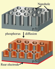
Silicon solar cells with arrays of nano-sized holes could outperform their nanowire-based rivals, say Chinese chemists. Nanohole arrays are less fragile and more efficient than nanowires, and can be manufactured using conventional techniques.
Kui-Qing Peng and colleagues from Beijing Normal University and City University of Hong Kong had been investigating silicon nanowire-based solar cells, but consistently hit problems. The high surface area and increased light absorption properties of nanostructured silicon makes it very attractive for solar cell applications, explains Peng, 'but nanowires are easily broken during solar cell fabrication and characterisation processes, so we switched to robust nanohole solar cells,' he says.

The cells are made by etching holes in silicon and coating them with a layer of doped silicon
© J. Am. Chem. Soc.
|
Nanohole arrays can absorb light even better than nanowire arrays - light that enters the holes will bounce around inside until it is absorbed. In nanowire cells, light is scattered and bounces between nanowires, but the holes seem to do a better job of capturing scattered photons, which increases their energy conversion efficiency. Zhong Lin Wang from the Georgia Institute of Technology in Atlanta, US, sees this as the main advantage of nanohole cells over nanowire. 'Such a structure could be very useful for enhancing the efficiency of silicon based solar cells,' Wang told Chemistry World.
Because the nanohole array is much less fragile than a forest of nanowires, it is also less susceptible to problems associated with broken nanowires, such as recombination of the electrons and positively charged 'holes' that carry current through the device, which boosts the cell's efficiency. Peng's cells can convert about 10 per cent of the solar energy shone on them into electricity, which is almost double that achieved by some of the best nanowire-based cells.
However, Peng is confident that they can easily push efficiency to 15 per cent or higher: 'All our present experiments are done in conventional labs, not clean rooms,' he says, 'and this efficiency was achieved with no effort put into efficiency-increasing modifications.' He adds that they are currently looking for industrial collaborators to help commercialise the discovery, and since conventional techniques are used to etch holes in silicon wafers and coat them with doped silicon to make the cell, they should be easily scalable for industrial application.
Phillip Broadwith
Interesting? Spread the word using the 'tools' menu on the left.


